
-
Engineering and Architecture
Exams
Colleges
Predictors
Resources
-
Computer Application and IT
Quick Links
Colleges
-
Pharmacy
Colleges
Resources
-
Hospitality and Tourism
Colleges
Resources
Diploma Colleges
-
Competition
Other Exams
Resources
-
School
Exams
Ranking
Products & Resources
-
Study Abroad
Top Countries
Student Visas
-
Arts, Commerce & Sciences
Exams
Colleges
Upcoming Events
Resources
-
Management and Business Administration
Exams
Colleges & Courses
Predictors
-
Learn
Online Courses
Engineering Preparation
Medical Preparation
-
Online Courses and Certifications
Top Streams
Specializations
- Digital Marketing Certification Courses
- Cyber Security Certification Courses
- Artificial Intelligence Certification Courses
- Business Analytics Certification Courses
- Data Science Certification Courses
- Cloud Computing Certification Courses
- Machine Learning Certification Courses
- View All Certification Courses
Resources
-
Medicine and Allied Sciences
Colleges
Predictors
Resources
-
Law
Resources
Colleges
-
Animation and Design
Animation Courses
Colleges
Resources
-
Media, Mass Communication and Journalism
Exams
Colleges
Resources
-
Finance & Accounts
Top Courses & Careers
Colleges
Get Answers to all your Questions


All Questions

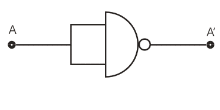
Boolean relation at the output stage - Y for the following circuit is :
Option: 1
Option: 2
Option: 3
Option: 4
The first part of the given circuit represents or gate whose output is A+B
The second part of the circuit is NOT gate whose input is A+B and output is
So the correct option is 4.
View Full Answer(1)The circuit shown below is working as a 8 V dc regulated voltage source . When 12 V is used as input, the power dissipated (in mW) in each diode is ; (considering both zener diodes are identical ) _____.
Option: 1 40
Option: 2 30
Option: 3 50
Option: 4 20


Crack CUET with india's "Best Teachers"
- HD Video Lectures
- Unlimited Mock Tests
- Faculty Support

Which of the following gives a reversible operation?
Option: 1 
Option: 2
Option: 3 
Option: 4 
For reversible operation, NOT gate is used. If an input isthen output=
. The following circuit represents the NOT gate
So Option (2) is correct.
View Full Answer(1)The current i in the network is : 
Option: 1
Option: 2
Option: 3
Option: 4
Both diodes are in reverse biased
So new circuits can be drawn as

So
Hence the correct option is (1).
View Full Answer(1)JEE Main high-scoring chapters and topics
Study 40% syllabus and score up to 100% marks in JEE
In the given circuit, the value of Y is : 
Option: 1 toggles between 0 and 1
Option: 2 1
Option: 3 0
Option: 4 will not execute

In NAND gate, when
Hence the correct option is (3)
View Full Answer(1)Both the diodes used in the circuit shown are assumed to be ideal and have negligible resistance when these are forward biased. Built-in potential in each diode is 0.7V. For the input voltages shown in the figure, the voltage (in Volts) at a point A is ______________ 
Option: 1 12
Option: 2 10
Option: 3 40
Option: 4 24
We want to find VE
By applying kvl in AEFBA

12.7 - 0.7 - VE = 0.
implies
VE = 12V
Hence the correct option is (1).
NEET 2024 Most scoring concepts
- Just Study 32% of the NEET syllabus and Score up to 100% marks
A transistor is connected in common emitter circuit configuration, the collector supply voltage is 10 V and the voltage drop across a resistor of in the collector circuit is 0.6 V. If the current gain factor
is 24, then the base current is _______
. (Round off to the Nearest Integer)
Find the truth table for the function  represented in the following figure.

Option: 1 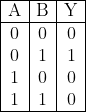
Option: 2 
Option: 3 
Option: 4 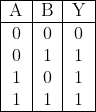

The correct option is (2)
View Full Answer(1)Crack CUET with india's "Best Teachers"
- HD Video Lectures
- Unlimited Mock Tests
- Faculty Support
Statement I:
By doping silicon semiconductor with pentavalent material,the electrons density increases.
Statement II :
The n-type semiconductor has net negative charge.
In the light of the above statements,choose the most appropriate answer from the options given below:
Option: 1 Both statement I and Statement II are false.
Option: 2 statement I is true but Statement II is false.
Option: 3 Statement I is false but Statement II is true.
Option: 4 Both Statement I and Statement II are true.
Statement I
By doping silicon semiconductors with pentavalent material.
Statement II
The n-type semiconductor has a net negative charge
Both the statements are true
Hence, the correct option is (4)
Identify the logic operation carried out by the given circuit :

Option: 1 OR
Option: 2 AND
Option: 3 NAND
Option: 4 NOR

The logic operation carried out in the above circuit is equivalent to NOR Gate
The correct option is (4)
JEE Main high-scoring chapters and topics
Study 40% syllabus and score up to 100% marks in JEE

